TSMC's Advanced Packaging Bottleneck: Can the Industry Keep Pace with AI Demand?
TSMC faces mounting pressure to scale advanced chip packaging technologies as AI accelerator demand outpaces production capacity. The semiconductor leader's CoWoS and other advanced packaging platforms are becoming critical constraints in the AI supply chain.
TSMC's Advanced Packaging Bottleneck: Can the Industry Keep Pace with AI Demand?
TSMC, the world's largest contract chipmaker, is confronting a significant constraint that threatens to limit AI chip availability: advanced packaging capacity. As demand for high-performance AI accelerators surges globally, the company's ability to package these complex multi-die systems is emerging as a critical bottleneck in the semiconductor supply chain.
The Packaging Challenge
Advanced packaging technologies—particularly 2.5D and 3D interconnect solutions—are essential for modern AI chips. These techniques stack multiple dies (processor cores, memory, and logic components) in compact configurations, enabling the high bandwidth and performance that large language models and AI inference systems demand. However, packaging is far more labor-intensive and capital-intensive than wafer fabrication alone.
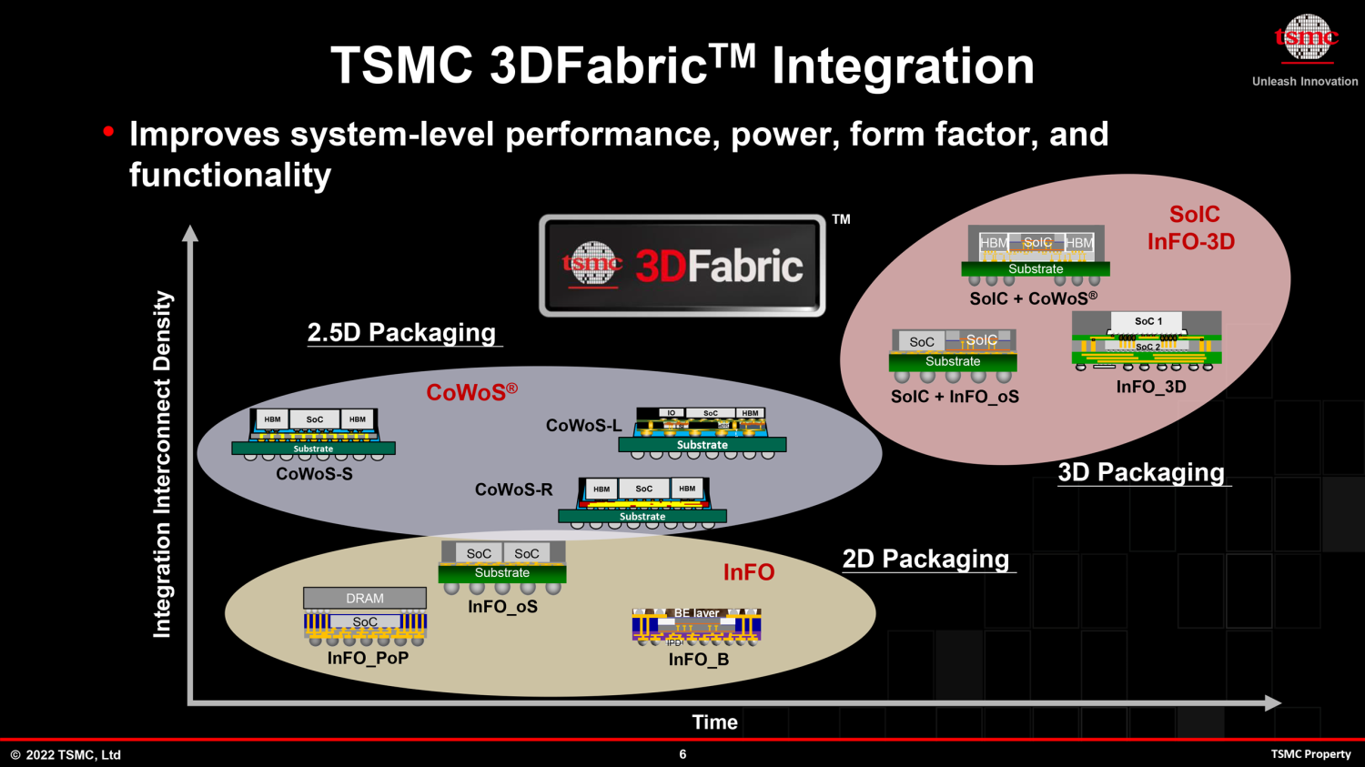
TSMC's CoWoS (Chip-on-Wafer-on-Substrate) platform represents the current industry standard for high-end GPU and AI accelerator packaging. This technology allows chipmakers to integrate GPU logic dies with high-bandwidth memory (HBM) stacks and interposers—a critical requirement for NVIDIA's H100 and H200 accelerators, as well as AMD's MI300 series. Yet CoWoS capacity has become increasingly constrained as AI adoption accelerates across cloud providers, enterprises, and research institutions.
Capacity Constraints and Market Impact
The gap between wafer production and packaging throughput has widened considerably. While TSMC can manufacture advanced process nodes at scale, the subsequent packaging, testing, and assembly steps cannot keep pace with demand. This creates a peculiar supply chain paradox: chips may be ready for packaging weeks or months before capacity becomes available.
Industry observers note that:
- CoWoS utilization rates have reached near-maximum levels, with some reports suggesting 90%+ capacity utilization
- Lead times for advanced packaging services have extended significantly, affecting customer delivery schedules
- Capital intensity of packaging facilities requires substantial investment, limiting rapid capacity expansion
- Yield challenges in advanced packaging add complexity to scaling operations
TSMC's Response and Expansion Plans
TSMC has announced plans to expand advanced packaging capacity, including investments in new facilities and process improvements. The company is also exploring alternative packaging technologies to distribute demand, including chiplet-based approaches that may reduce reliance on the most advanced (and capacity-constrained) packaging nodes.
However, expansion timelines are measured in years, not quarters. New packaging facilities require significant construction, equipment installation, and process validation before they can contribute meaningful capacity to the market.
Broader Industry Implications
The packaging bottleneck has broader implications for the AI ecosystem:
- GPU availability remains constrained despite increased wafer starts
- Customer allocation decisions increasingly hinge on packaging capacity rather than wafer production
- Alternative suppliers including Samsung and Intel are investing in advanced packaging to capture market share
- Chiplet strategies are gaining traction as a workaround to reduce advanced packaging dependencies
Key Sources
The semiconductor industry's understanding of TSMC's packaging challenges comes from supply chain analysis, investor communications, and technical publications tracking advanced packaging trends. Industry analysts and semiconductor equipment manufacturers have documented the growing disparity between wafer production capacity and packaging throughput, particularly for AI-focused applications.
Looking Ahead
TSMC's packaging constraints underscore a critical vulnerability in the AI supply chain. While the company maintains technological leadership in advanced packaging, the sheer magnitude of AI demand may exceed what current and near-term capacity can support. This dynamic will likely shape chip availability, pricing, and customer relationships throughout 2024 and beyond.
The resolution of this bottleneck will require coordinated efforts across TSMC's operations, potentially including process innovations, capacity investments, and strategic partnerships with packaging specialists. Until then, advanced packaging remains the constraint that limits how quickly the semiconductor industry can satisfy the world's appetite for AI compute.


